Today, you probably asked a question of a large language model, or accepted a connection suggestion on LinkedIn, or watched a recommended video on YouTube, or took a different route to work based on a traffic prediction from Google Maps. In other words, you probably used artificial intelligence. But what you might not know is how much energy that interaction consumed or why.
AI requires processing massive amounts of data, which is usually done in large data centers populated by thousands of GPUs capable of executing up to trillions of operations per second. But each of those GPUs achieves that by consuming as much as 1,000 watts apiece. For comparison, if you’ve got a newer smartphone, it probably uses less than 1 W. That kilowatt figure puts GPUs on the same level as vacuum cleaners, dishwashers, and stoves, but with the big difference that data-center processors are operating uninterrupted around the clock.
Fundamentally, a lot of this inefficiency is because GPUs are trying to simulate the workings of artificial neural networks using software and billions of transistors, which requires using energy to move massive amounts of data. What’s more, the simulated artificial neurons that make up these networks lack even a fraction of the complex computing behavior of the biological neurons that comprise the most energy-efficient computing system that we know, the human brain.
The brain is roughly one million times as energy efficient at many of the comparable tasks we set for AI. To try to approach these efficiencies, a radically different way of computing called neuromorphic engineering is seeking to build electronic components and circuits that act more like the brain’s neurons and the synapses that connect them.
Huge amounts of work have gone into making electronics operate more like biological neurons and synapses. Some research has focused on developing new, experimental devices, but they aren’t yet reliable enough to be used in large systems. Other efforts aim to implement neurons and synapses by interconnecting many complementary metal-oxide-semiconductor (CMOS) transistors—the workhorses of digital logic—to simulate a single neuron and synapse. But this approach requires so many transistors (and a few bulky capacitors) that it greatly limits the size of the system that can be constructed, making it unclear how such brain-inspired hardware could ever scale up and compete with state-of-the-art GPUs.
But all along there was an artificial neuron and a synapse—each a single device—hiding in plain sight. We found them last year. They were each made possible by an ordinary CMOS transistor—and not even a very good one at that. This is the story of their accidental discovery and their great promise for lowering the environmental footprint of AI.
Biological and artificial neurons
Modern digital electronics is based on producing and manipulating the ones and zeros of the binary code through the operation of metal-oxide-semiconductor field-effect transistors. MOSFETs have evolved in recent years, but their classic form consists of a piece of silicon that has been doped to contain an excess of either positive (p-type) or negative (n-type) charge carriers. (CMOS logic contains transistors of both types.) The device has two terminals connected to the silicon through regions highly doped with the opposite polarity of the rest of the silicon—the source and the drain. Another terminal, the gate, sits atop the silicon that separates the source from the drain. The gate itself doesn’t connect directly to this silicon, instead resting above a thin layer of insulating dielectric.
Notably, there is a fourth terminal that attaches to the bulk of the silicon; think of this bulk terminal as connecting to the underside of the chip. It doesn’t typically get much attention, but it’s very important to our story.
When voltage is applied at the gate and the bulk terminal is grounded, charge carriers of the same polarity as the source and drain are attracted to the channel region. In the case of an n-type source and drain, that will be electrons; for p-type it will be holes. The presence of these charges forms a conductive channel that reduces the resistance between the source and the drain by several orders of magnitude, and the device switches on. As the voltage at the gate increases, this physical phenomenon produces a current signal that, when plotted against the gate voltage, rises steadily. This response is ideal for logic gates, converters, multiplexers, memories, and other digital circuits. But it is not a good fit for mimicking the behavior of a neuron.
In real neural tissue, brain cells, called neurons, consist of a cell body, a long projection called an axon, and short branching projections called dendrites. The suite of behaviors and computing this collection of components is capable of is rich and broad, but the portion that artificial neural networks hope to copy is this: When the cell body’s voltage is perturbed enough to reach a particular threshold, a self-propagating pulse of voltage, called an action potential, shoots down the axon. The axon terminates in a synapse, an electrochemical connection between the axon and another neuron’s dendrites. The action potential will then temporarily boost the voltage of this next neuron, by an amount that depends on the strength of the synaptic connection. If enough action potentials reach these dendrites in a given time—from this neuron or from others that might also form synapses there—the cell body’s voltage will surpass the threshold and trigger its own action potential.
The MOSFET Neuron
The unusual action the authors discovered is understandable if you consider that a MOSFET contains a hidden bipolar-junction transistor.
TRANSISTOR BEHAVIOR
Under normal operation, with the bulk terminal grounded, increasing voltage at the drain leads to current that increases steadily. When the voltage decreases, current follows the same sloped path. Although some pairs of electrons and holes are created by current crashing into silicon atoms, these are swept away before they can accumulate.
NSRAM BEHAVIOR
Adding resistance to the bulk terminal means these extra holes pile up, increasing the bulk voltage relative to the source. Once that voltage reaches a certain value, the hidden transistor activates, causing current to spike. Current remains high until the drain voltage drops past a certain point.
To get closer to the behavior of real neurons, artificial neurons should produce a current spike when a critical voltage threshold is crossed and then quickly relax back to a resting state on their own. This spike needs to be sudden—nonlinear. It should also exhibit some hysteresis; that is, the activation and relaxation voltages should be different from each other to ensure that current flows only for a certain amount of time.
What’s wanted from an artificial synapse, the thing that connects two artificial neurons, is less complicated, but equally important. The main thing is that its conductance can be electronically adjustable. The device’s conductive states should increase and decrease in a linear pattern and remain stable over time.
No single MOSFET working under the standard operation mechanism can reproduce either of these neural properties. Instead, it’s been done by combining them into complex circuits. Until now, each neuron and each synapse has been implemented by interconnecting dozens and sometimes even hundreds of MOSFETs, which is highly inefficient in terms of area, performance, and cost. To limit the amount of space needed, chips can multiplex their signals, sending them to neurons and synapses serially, but such sequential processing introduces additional delays.
Despite these area-and-time penalties on tasks such as audio processing, computer vision, or health monitoring, state-of-the-art brain-inspired microchips have achieved power reductions up to a thousandfold compared with those of GPUs or CPUs on the same task. If we could create neurons and synapses from individual devices that are readily manufacturable instead, we might target more massive implementations while maintaining energy efficiency.
Reinventing the MOSFET for AI
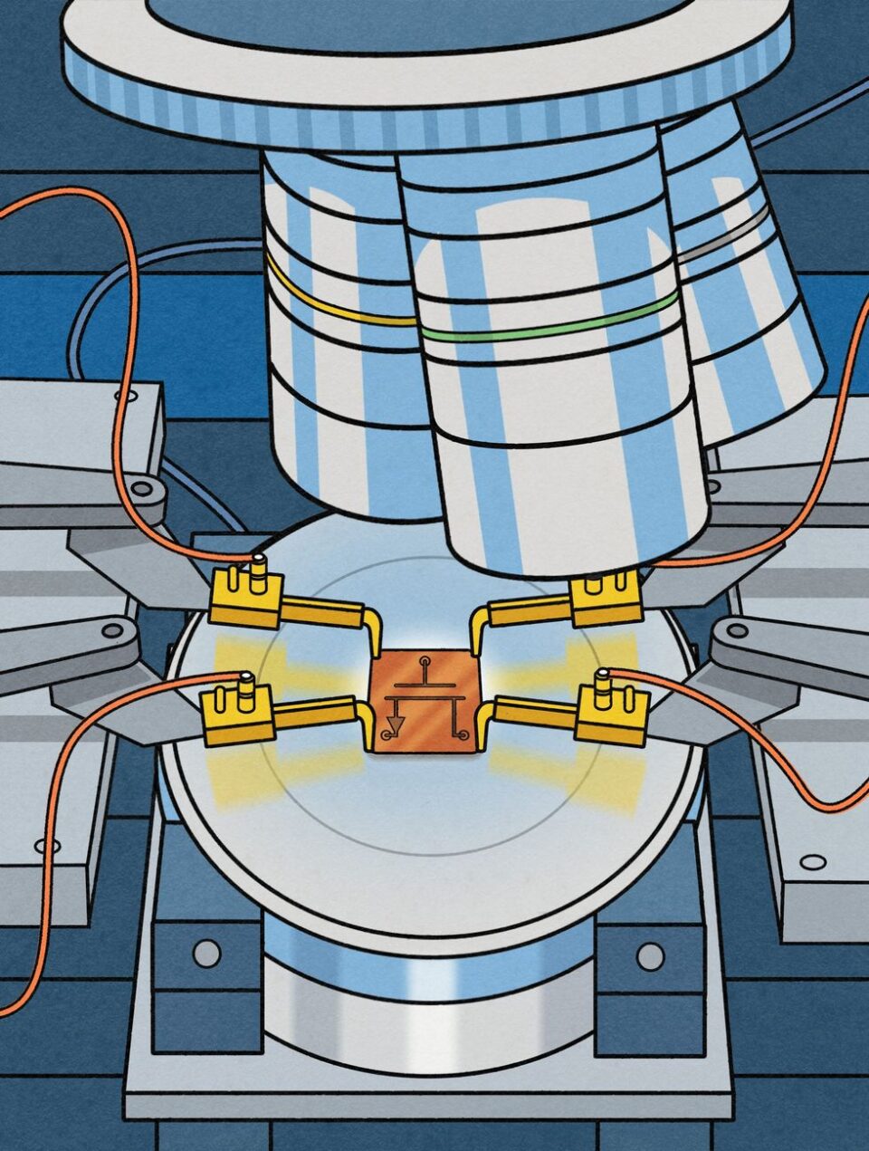
Working in our laboratory in 2024, one of my students was measuring a memory circuit that consisted of one transistor and one memristor—a type of nonvolatile memory device first fabricated in 2008. The student’s memristor circuit was built from two-dimensional material atop a silicon microchip containing MOSFETs. The MOSFETs were created in a commercial foundry using fabrication technology called the 180-nanometer node, which was cutting-edge in the year 2000.
One day the student forgot to connect the bulk terminal of the transistor. What he observed was a sudden increase in current with high nonlinearity that self-relaxed when the voltage was ramped down (a phenomenon called a hysteresis loop). This was a very promising neuronlike behavior!
After a fruitless week of trying to think of an explanation for this behavior, I (Lanza) asked Pazos, then my postdoctoral fellow, to try to observe and control this phenomenon in chips without memristors. This time, we applied pulses of voltage—like the spikes a neuron would produce—instead of the ramped voltage that my student used when he first saw the peculiar behavior.
Pazos’s new data helped us understand what was going on. The key was that oft-ignored fourth, or bulk, terminal of a MOSFET. Under ordinary operation, many mobile charge carriers flitting through the channel collide with the silicon atoms, producing free pairs of electrons and holes—a process known as impact ionization. The electric field created by the potential difference between the source and the drain causes these new free electrons to drift toward the positively biased drain and the holes to move toward the bulk terminal, which is usually grounded, removing the charge without any drama.
However, when the bulk terminal of the transistor is floating—unconnected as it was in my student’s experiment—the holes produced by impact ionization cannot be driven to the ground. Instead, they accumulate in the bulk of the silicon, increasing its voltage. Then things start to get interesting.
It helps here to imagine a MOSFET as two different kinds of transistors occupying the same physical space—the intentionally constructed MOSFET and a hidden, bipolar junction transistor. A bipolar device transmits a current signal across two p-n junctions, in this case the interfaces between the source and the channel region and the channel and the drain. This signal is in proportion to a smaller current at a third terminal in between, called the base. In our experiment, that third terminal is the bulk.
To get current flowing through a bipolar transistor, you need a big enough potential difference between the base and one of the other terminals, so that current can get across the p-n junction. Let’s say this “threshold voltage” is 0.7 volts, although the real number depends on device geometry and silicon doping. In our device, that potential difference comes from those holes that were accumulating in the bulk, because it was not connected to ground. Once it reaches the threshold voltage, the device becomes sharply conductive, producing an abrupt increase of current. This sharp current increase eventually falls off once the drain voltage is lowered, because that lowering reduces the rate at which holes are generated in the bulk. The remaining excess holes recombine with stray electrons or leak away, and finally the bulk voltage falls. This cycle of hole accumulation, current spike, and hole removal gives rise to a hysteresis loop, very much like the electrical behavior of a biological neuron as it integrates ionic currents, fires a spike, and relaxes back to its resting voltage.
Initially, we observed this behavior only in a few transistors, and the relaxation time was very different for each of them. So, to try to control it better, we adjusted the resistance of the bulk terminal using a second MOSFET. Simply setting that resistance suddenly caused all the transistors to fire at the same voltage with hardly any variability. In other words, we found we could create perfect electronic neuron behavior in a single silicon transistor by controlling the bulk contact resistance. Setting the resistance can be done by doping the silicon during fabrication, but we think the two-transistor cell—where one acts as the bulk resistance—offers much greater versatility because it allows for electronic control.
We had to make sure the phenomenon would last, otherwise such a device would be useless. To our delight, every single one of the devices we tested worked over 10 million cycles. Not even one of them failed during our tests.
The MOSFET Synapse
To be honest, we were amazed. Dozens of research groups and companies all around the world have spent many millions of U.S. dollars over the past 20 years trying to emulate these neural behaviors using experimental memristor-like devices and other things, with limited success, mainly due to reliability and cost issues. We managed it in the cheapest and most industry-standard device: the MOSFET. This result was so shocking that we decided to confirm it using microchips from a different foundry. It was successful: All the behaviors could be reproduced, and perfect yield was achieved once again.
We were happy with the results and had started the process of filing for a patent and writing up our findings for the journal Nature, when our lab made another astonishing discovery: The same kind of MOSFET could act as a synapse, too!
Recall that in ordinary operation some electrons crash into silicon atoms to create pairs of electrons and holes. We noticed that at specific values of bulk resistance a significant amount of the charge from this impact ionization would get trapped in the gate dielectric. This trapped charge interferes with the flow of current through the MOSFET, effectively changing the device’s conductance. Importantly, this new conductance is stable and adjustable at will. It was then that we realized the MOSFET could also be used as an electronic synapse.
As it was in the neuron transistor, the bulk terminal was the key. A negative bulk-source voltage drives electrons into the dielectric, decreasing conductance. A positive one pushes holes in, increasing it.
From neuromorphic device to circuit to system
Here’s how the MOSFET synapse and the MOSFET neuron, together called a neurosynaptic random-access memory, or NSRAM, could work together to achieve a simple neural circuit: Say you had a circuit consisting of three synapse MOSFETs and a neuron MOSFET. The synapses have already been programmed as we’ve described, so that each has a different conductance. Spikes of voltage with different patterns and frequencies are applied to the gate of each of these transistors. What emerges from their drains are spikes of current with amplitudes modulated by the synapses conductance values.
The spikes converge at the drain of the neuron MOSFET. With each spike, impact ionization causes charge to build in the bulk of the silicon. Some of it will drain away, but if enough spikes arrive in a short enough period of time, the bulk voltage will reach a value at which the “hidden” transistor triggers a spike of current through the MOSFET. This current would then go on to become the input to other MOSFET synapses, and so on. The behavior is exactly the kind of integrate-and-fire action real neural circuits deliver.
The competitive advantage of our single-MOSFET electronic neurons and synapses is straightforward: We can produce with only one or two transistors the electronic signals that today require, at an industrial level, dozens and sometimes even hundreds of components. And moreover, unlike other emerging technologies, our solution is fully compatible with today’s silicon manufacturing lines and exhibits a yield of 100 percent in key figures of merit with near-zero variability.
Building functional circuits for brain-inspired computing and AI based on this technology is as exciting as it is laborious. It will require us to improve our computer models to resemble the behavior of both devices more accurately and to do so with computational efficiency. We must also perform accurate circuit- and system-level simulations to validate computing architectures, design peripheral circuitry to drive and convert signals, and undergo multiple fabrication rounds to optimize performance.
But all that will be worthwhile, because it could result in brain-inspired microchips for AI with better energy efficiencies than what we have now. These chips will first be a fit for smaller-scale, “edge-AI” tasks, such as bringing greater intelligence to battery-powered systems. But if we can scale up such chips, maybe in the long run they can compete with state-of-the-art GPUs.